A low-disorder metal-oxide-silicon double quantum dot

Publication Year
2019

Type

Journal Article
Abstract
One of the biggest challenges impeding the progress of Metal-Oxide-Silicon (MOS) quantum dot devices is the presence of disorder at the Si/SiO\$\_2\$ interface which interferes with controllably confining single and few electrons. In this work we have engineered a low-disorder MOS quantum double-dot device with critical electron densities, i.e. the lowest electron density required to support a conducting pathway, approaching critical electron densities reported in high quality Si/SiGe devices and commensurate with the lowest critical densities reported in any MOS device. Utilizing a nearby charge sensor, we show that the device can be tuned to the single-electron regime where charging energies of \$\backslashapprox\$8 meV are measured in both dots, consistent with the lithographic size of the dot. Probing a wide voltage range with our quantum dots and charge sensor, we detect three distinct electron traps, corresponding to a defect density consistent with the ensemble measured critical density. Low frequency charge noise measurements at 300 mK indicate a 1/\$f\$ noise spectrum of 3.4 \$\backslashmu\$eV/Hz\$\^\1/2\\$ at 1 Hz and magnetospectroscopy measurements yield a valley splitting of 110\$\backslashpm\$26 \$\backslashmu\$eV. This work demonstrates that reproducible MOS spin qubits are feasible and represents a platform for scaling to larger qubit systems in MOS.
Journal
Applied Physics Letters
Volume
114
Pages
043501
ISSN Number
00036951

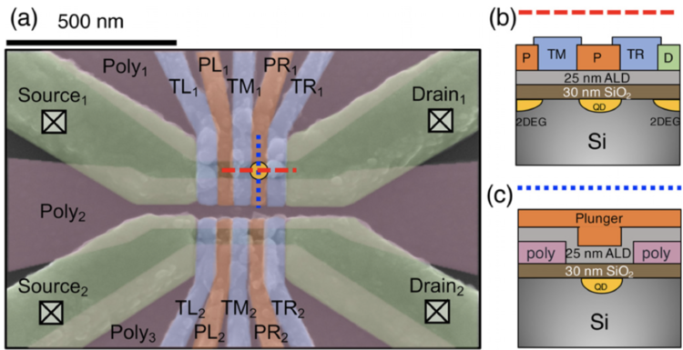
One of the biggest challenges impeding the progress of metal-oxide-silicon (MOS) quantum dot devices is the presence of disorder at the Si/SiO2 interface which interferes with controllably confining single and few electrons. In this work, we have engineered a low-disorder MOS quantum double-dot device with critical electron densities, i.e., the lowest electron density required to support a conducting pathway, approaching critical electron densities reported in high quality Si/SiGe devices and commensurate with the lowest critical densities reported in any MOS device. Utilizing a nearby charge sensor, we show that the device can be tuned to the single-electron regime where charging energies of 􏰃8 meV are measured in both dots, consistent with the lithographic size of the dot. Probing a wide voltage range with our quantum dots and charge sensor, we detect three dis- tinct electron traps, corresponding to a defect density consistent with the ensemble measured critical density. Low frequency charge noise measurements at 300 mK indicate a 1/f noise spectrum of 3.4 leV/Hz1=2 at 1 Hz and magnetospectroscopy measure- ments yield a valley splitting of 110 6 26 leV. This work demonstrates that reproducible MOS spin qubits are feasible and repre- sent a platform for scaling to larger qubit systems in MOS.